Custom Analog
IC Design.Schematic to Layout
Build practical analog IC design skills through a three-month, full-time Train & Place programme, with hands-on training, career preparation, and job placement.
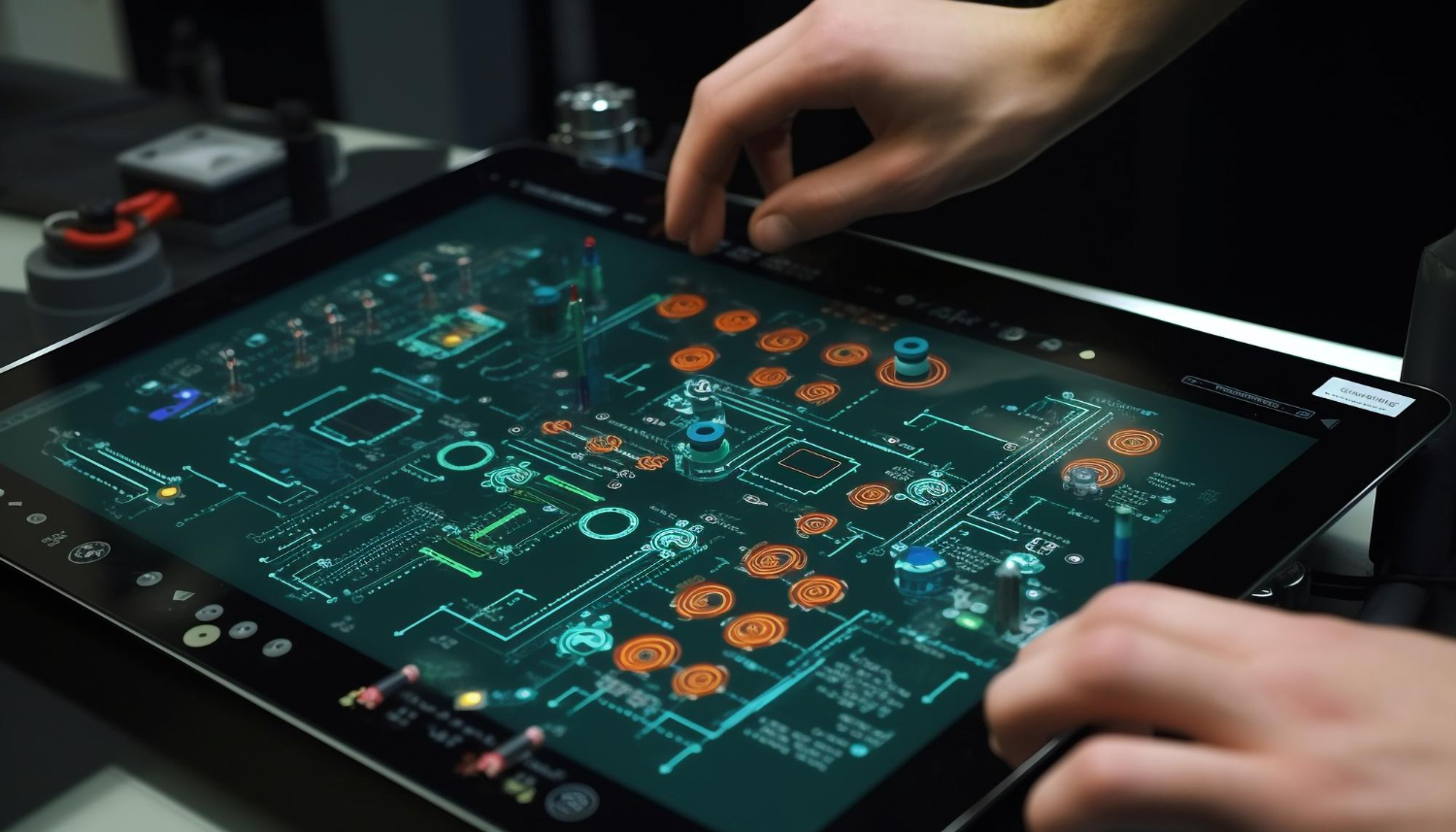

Design. Simulate.
Bring your ideas to silicon.
- Programme duration
- 3 months
- Commitment
- Full-time
- Training format
- Face-to-face
Turn theory into design.
Custom Analog IC Design: Schematic to Layout is a Professional Skills Train & Place Programme for high-demand careers. Develop practical analog CMOS design skills through three months of full-time intensive training, supported by industry-standard Electronic Design Automation (EDA) tools.
The full custom IC design flow
Explore MOS models, CMOS technologies and layouts, amplifiers, current mirrors, and precision reference circuits. Each technical chapter includes a lab exercise. Alongside technical training, build communication, work ethics, and presentation skills, then progress to job interviews with companies through the programme’s job placement stage.
Course objectives
- Analyze and apply theoretical concepts of analog CMOS VLSI circuit design.
- Integrate and design analog CMOS VLSI circuits using innovative techniques.
- Evaluate CMOS circuit performance using industry-standard EDA tools.
- Understand the end-to-end process of IC design, from modeling to layout and verification.
Build skills for the whole design flow.
What you’ll be able to do
- Explain core principles of analog CMOS VLSI circuit design.
- Design, simulate, and verify analog CMOS circuits using modern techniques.
- Apply circuit optimization strategies to meet performance and area constraints.
- Use industry-standard EDA tools for circuit simulation, layout, and verification.
- Apply circuit design concepts through practical lab exercises.
Skills you’ll develop
- Analog CMOS circuit design.
- Semiconductor device modeling (MOSFETs, diodes, current mirrors).
- Industry-standard EDA tools and circuit simulation environments.
- Layout design and verification (DRC, LVS, PEX).
- Problem-solving in high-performance circuit design.
- Innovation in application-specific IC development.
Focus on your skills. We’ll support the journey.
The programme combines technical training with practical support during the three-month training period.
RM1,500
Every month during the three-month training programme.
A place to stay
Accommodation provided during the three months of training.
1 year
One-year insurance coverage is included as a programme benefit.
Training & career benefits
- Face-to-face training
- Soft skills & career readiness training
- Hands-on practical training
- Industry-standard EDA tools
- Industry-relevant skills & exposure
- Job placement provided
- Professional career pathway
From MOS models to operational amplifiers.
Nine technical chapters with lab exercises, complemented by soft skills development and career readiness training.
01Introduction to MOS Models
- Fundamentals of MOSFET Operation and Characteristics
- Analytical Techniques for MOSFET Modeling
- Small-Signal Model Derivation and Application for MOS Transistors
- Comprehensive Modeling of Internal and External Parasitics
- Lab Exercise
02CMOS Technologies and Layouts
- CMOS Technology Overview and Fabrication Process
- Detailed Physical Layout Techniques for MOS Transistors
- Verification Processes: Design Rule Checking (DRC), Parasitic Extraction (PEX), and Layout Versus Schematic (LVS)
- Methods for Optimizing Silicon Utilization and Layout Efficiency
- Lab Exercise
03CMOS Diodes and Active Resistors
- Overview of CMOS Diodes: Structure and Functionality
- Modeling Approaches and Analysis Techniques for CMOS Diodes and Active Resistors
- Design Trade-offs and Constraints in CMOS Diodes and Resistors
- Lab Exercise
04CMOS Single-Stage Amplifiers
- Introduction to Single-Stage Amplifier Configurations and Principles
- Design and Analysis of Common-Source, Source Follower, and Common-Gate Amplifiers
- Effects of Loading on Amplifier Performance and Stability
- Analyzing Trade-offs and Performance Optimization in Single-Stage Amplifiers
- Lab Exercise
05Basic and High Output Impedance Current Mirrors
- Principles of Current Mirror Circuits and Their Applications
- Design and Analysis of Widlar and Cascode Current Mirror Configurations
- Impact of Current Mirror Design on Amplifier Loading and Performance
- Evaluating Trade-offs in High Output Impedance Current Mirror Designs
- Lab Exercise
06CMOS Differential Pair and Cascode Amplifiers
- Introduction to Differential Pair and Cascode Amplifier Concepts
- Detailed Design and Analysis of Differential Amplifiers
- Implementation and Analysis of Differential Amplifiers Using Current Mirrors
- Stability Compensation Techniques for Differential and Cascode Amplifiers
- Evaluating Performance Trade-offs in Differential and Cascode Amplifiers
- Lab Exercise
07CMOS Current, Output, and High-Gain Amplifiers
- Introduction to Current, Output, and High-Gain Amplifier Concepts
- In-Depth Design and Performance Analysis of Current, Output, and High-Gain Amplifiers
- Lab Exercise
08CMOS Precision Voltage and Current Reference Circuits
- Introduction to Precision Voltage and Current Reference Circuits
- Design Principles and Analytical Methods for Precision Voltage and Current References
- Lab Exercise
09Design and Compensation of CMOS Operational Amplifiers
- Introduction to Operational Amplifier Design Principles
- Techniques for Pole-Zero Splitting and Compensation in Operational Amplifiers
- Design Methodologies and Analytical Techniques for Operational Amplifiers
- Lab Exercise
Soft Skills Development
- Communication Essential Skills
- Work Ethics Skills
- Presentation Skills
Build your next career in IC design.
Eligibility
- Malaysian Bumiputera
- 22 to 35 years old
Who this programme is for
- Fresh graduates with a Bachelor’s or Master’s Degree in Electrical & Electronic Engineering
- Unemployed engineers transitioning to IC design
Certificates
Certified byCity & Guilds
Training completion
Certificate of Training Completion in Custom Analog IC Design: Schematic to Layout
Programme completion
Certificate of Programme Completion in Custom Analog IC Design: Schematic to Layout (Train & Place)
Soft skills training
Certificate of Completion (Soft Skills Training)
Register. Train. Take the next step.
Registration
Register via the e-form, attend an interview session by MASET, and join the cohort orientation briefing.
Train & Place
Complete three months of full-time intensive training, followed by completion of training and certificate award.
Job placement
Progress to job interviews with companies as part of the programme’s job placement stage.
Explore your path in semiconductors.
Prepare for a professional career pathway through industry-relevant skills, hands-on technical experience, soft skills, and career readiness training. Job placement is provided as part of the Train & Place programme, with job interviews with companies following training.
Career roles & progression
The occupational structure within the semiconductor industry consists of various job levels, ranging from entry-level technicians to advanced IC design engineers. The primary job area covered in this program is Custom IC Design, which involves the design, simulation, and validation of integrated circuits. The structure includes the following levels:
- Assists in basic circuit layout, PCB design, and simple testing.
- Works under the supervision of senior engineers.
- Develops foundational knowledge in semiconductor devices and fabrication.
- Engages in circuit design and analysis with guidance from senior engineers.
- Gains experience with Electronic Design Automation (EDA) tools.
- Assists in debugging and verifying circuit performance.
- Conducts advanced IC design, simulation, and troubleshooting.
- Works on complex circuits, optimizing performance and power consumption.
- Coordinates with fabrication teams for manufacturing.
- Leads design projects and optimizes circuit performance.
- Works on advanced simulation techniques and verification processes.
- Provides mentorship to junior engineers.
- Oversees multiple design projects and ensures compliance with industry standards.
- Develops new methodologies for circuit design and verification.
- Manages collaboration between design, fabrication, and testing teams.
- Focuses on cutting-edge technology development in semiconductors.
- Engages in exploratory research for next-generation ICs.
- Works in collaboration with universities and research institutions.
Industry competencies
Professionals in this field must possess a strong understanding of MOS models, CMOS technologies, and circuit design principles. Key competencies include:
- MOSFET Knowledge: Understanding MOSFET operation, modeling techniques, and electrical characteristics.
- CMOS Circuit Design: Designing and analyzing CMOS circuits such as amplifiers, current mirrors, and voltage references.
- Fabrication Processes: Implementing semiconductor fabrication processes, including photolithography, doping, and etching.
- EDA Tools: Utilizing electronic design automation (EDA) tools for circuit simulation, layout, and verification.
- Compliance Standards: Ensuring compliance with industry standards such as IEEE, JEDEC, and ISO guidelines.
- Troubleshooting: Troubleshooting design issues and optimizing performance for power efficiency and stability.
The working environment
The work environment in the semiconductor industry varies depending on job roles. Common working conditions include :-
- Laboratory and cleanroom settings requiring adherence to strict safety and contamination protocols.
- Use of specialized software for circuit simulation, layout, and verification, such as Cadence Virtuoso and Synopsys tools.
- Collaboration with multidisciplinary teams, including design, process, and test engineers.
- Adherence to strict deadlines and project timelines to meet industry demands.
- Continuous learning to keep up with technological advancements and industry trends.
- High precision and accuracy in testing and fabrication to minimize defects and improve yield.
- Exposure to hazardous materials requiring proper safety measures, including the handling of chemicals used in semiconductor processing
Employment prospects
The demand for skilled semiconductor professionals continues to grow due to the rapid expansion of the electronics, telecommunications, and computing industries. Employment opportunities exist in :-
- Semiconductor manufacturing companies, including major players like Intel, TSMC, and Samsung.
- Research and development institutions focusing on next-generation IC technologies.
- Telecommunications and consumer electronics industries developing cutting-edge devices.
- Automotive and medical device sectors requiring specialized semiconductor components.
- Academia and technical training institutions providing education and research opportunities.
- Startups and innovation centers working on emerging semiconductor applications.
Other position in semiconductor physical design engineering :
- IC Design Engineer.
- Physical Design Engineer.
- Senior IC Design Engineer.
- Senior Physical Design Engineer.
Learn from experience.

Dr. Harikrishnan Ramiah
Recipient of the Top Research Scientists Malaysia (TRSM) Award 2025 from the Academy of Sciences Malaysia (ASM), in Integrated Circuits (IC) Design.
Harikrishnan Ramiah received the B.Eng. (Hons), M.Sc., and Ph.D. degrees in electrical and electronic engineering, in the field of analog and digital IC design, from Universiti Sains Malaysia, Malaysia.
View trainer profileTalk to the programme team.
For programme enquiries, contact Syafeq or the MASET and TEC team.
[email protected]
[email protected]
Office address
Unit SS-G-08 SkyPod Square,Persiaran Puchong Jaya Selatan,
Bandar Puchong Jaya,
47100 Puchong, Selangor
About MASET & TEC
Malaysian Association of Science and Engineering Technology (MASET)
MASET is a professional training and development organisation focused on advancing industry-relevant skills through professional certification, upskilling and reskilling programmes.
Telecommunication Engineering College (TEC)
TEC is a Technical and Vocational Education and Training (TVET) institution focused on developing practical and technical capabilities aligned with industry needs.
Your ideas. Your next circuit.
Join three months of full-time technical and soft skills training, with a monthly stipend, accommodation during training, one-year insurance coverage, and a Train & Place career pathway.